Abse2001/OR-Gate-Tutorial
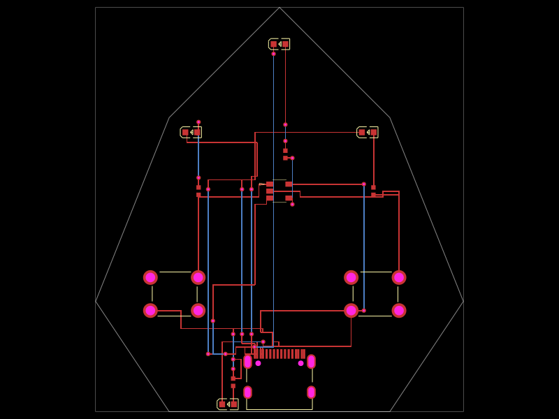
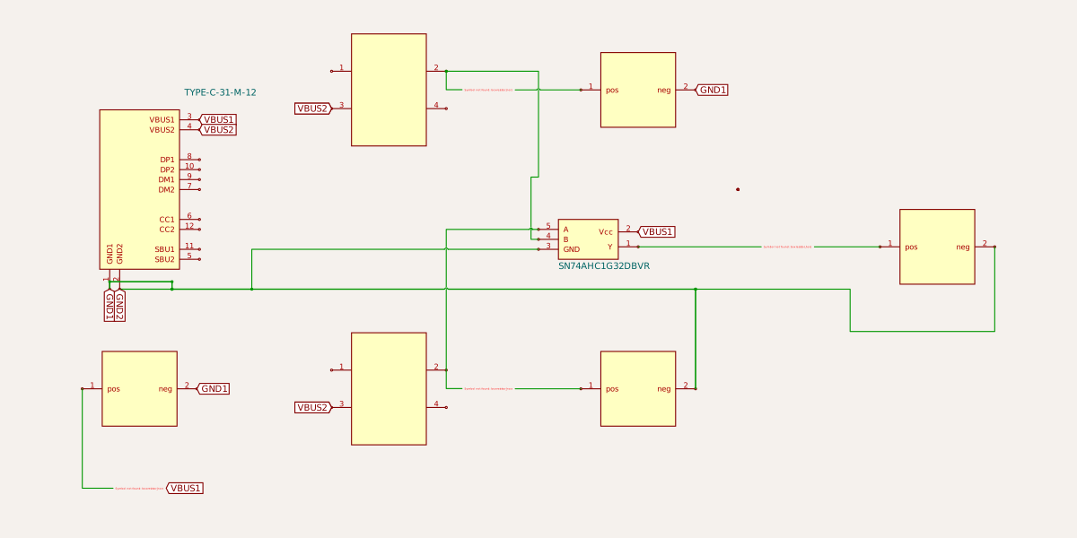
A USB-C powered circuit with two push buttons controlling four red LEDs and an OR gate to combine button signals.
Usage: To import and use the OR Gate component: ```tsx import { useOrGate } from "@tsci/Abse2001.OR-Gate-Chip" // In your component: const OR = useOrGate("OR") // Then use in a board, referencing its pins <board> <OR schY={-1} schX={-3} /> {/* Connect to specific pins */} <trace from={OR.pin2} to="net.VBUS1" /> <trace from={OR.pin4} to={someOtherComponent.pin} /> </board> ``` Key points: - Import from "@tsci/Abse2001.OR-Gate-Chip" - Use `useOrGate()` to create an instance - Passes name as argument - Can position with `schX/schY` - Pins can be referenced like `OR.pin2`, `OR.pin4`, etc.
- Version
- 0.0.1
- License
- unset
- Stars
- 0
index.ts
PCB
Schematic
import { useRedLed } from "@tsci/seveibar.red-led"
import { usePushButton } from "@tsci/seveibar.push-button"
import { useUsbC } from "@tsci/seveibar.smd-usb-c"
import { useOrGate } from "@tsci/Abse2001.OR-Gate-Chip"

export default () => {
  const B1 = usePushButton("B1")
  const B2 = usePushButton("B2")
  const USBC = useUsbC("USBC")
  const LED1 = useRedLed("LED1")
  const LED2 = useRedLed("LED2")
  const LED3 = useRedLed("LED3")
  const LED4 = useRedLed("LED4")
  const OR = useOrGate("OR")

  return (
    <board
      outline={[
        { x: -15, y: -30 },
        { x: 15, y: -30 },
        { x: 25, y: -15 },
        { x: 15, y: 10 },
        { x: 0, y: 25 },
        { x: -15, y: 10 },
        { x: -25, y: -15 },
        { x: -15, y: -30 },
      ]}
      width="30mm"
      height="60mm"
    >
      <USBC GND1="net.GND1" GND2="net.GND2" VBUS1="net.VBUS1" VBUS2="net.VBUS2" schY={0} schX={-12} pcbY={-24.6} />
      <B1 schY={-4} schX={-7} pcbY={-14} pcbX={-14.3} />
      <B2 schY={2}  schX={-7} pcbY={-14} pcbX={13} />

      <resistor
        name="R1"
        schY={-4}
        schX={-5}
        pcbRotation="90"
        pcbX={-11}
        resistance="150"
        footprint="0402"
      />
      <resistor
        name="R2"
        pcbRotation="90"
        pcbX={12.77}
         schY={2}
        schX={-5}
        resistance="150"
        footprint="0402"
      />
      <resistor
        name="R3"
        pcbRotation="90"
        pcbX={0.8}
        pcbY={5}
         schY={-1.15}
         schX={1}
        resistance="150"
        footprint="0402"
      />
      <resistor
        name="R4"
        pcbRotation="90"
        pcbY={-26}
        pcbX={-6.3}
        schY={-6}
        schX={-12}
        resistance="150"
        footprint="0402"
      />
      <LED1 schY={-4} schX={-2} pcbY={8} pcbX={-12} />
      <LED2 schY={2} schX={-2} pcbY={8} pcbX={12} />
      <LED3 schY={-1.15} schX={4} pos={OR.pin2} pcbY={20} pcbX={0} />
      <LED4 schY={-4} schX={-12} pcbY={-29} pcbX={-7} />
      <OR schY={-1} schX={-3} />

      <trace
        pcbRouteHints={[{ x: -13.4, y: -18.7 }]}
        from={B1.pin3}
        to="net.VBUS1"
      />
      <trace
        pcbRouteHints={[{ x: -13.4, y: -18.7 }]}
        from={B1.pin3}
        to="net.VBUS2"
      />
      <trace

        from=".B2 > .pin2"
        to=".OR > .pin4"
      />
      <trace

        from=".B2 > .pin2"
        to=".R2 > .pin1"
      />
      <trace from={B1.pin2} to=".R1 > .pin1" />
      <trace from=".B1 > .pin2" to=".OR > .pin5" />
      <trace from=".B2 > .pin3" to="net.VBUS1" />
      <trace from=".B2 > .pin3" to="net.VBUS2" />


      <trace from=".LED1 > .neg" to=".USBC > .GND2" />
      <trace from=".LED1 > .neg" to=".USBC > .GND1" />
      <trace from=".LED1 > .pos" to=".R1 > .pin2" />
      <trace from=".LED2 > .pos" to=".R2 > .pin2" />
      <trace from=".LED2 > .neg" to="net.GND1" />
      <trace from=".LED3 > .pos" to=".R3 > .neg" />
      <trace from=".R4 > .pos" to=".LED4 > .pos" />

      <trace

        from=".USBC > .GND2"
        to=".LED3 > .neg"
      />

      <trace from=".OR > .pin2" to="net.VBUS1" />
      <trace from=".OR > .pin1" to=".R3 > .pos" />
      <trace from=".OR > .pin3" to=".USBC > .GND1" />
      <trace from="net.VBUS1" to=".R4 > .neg" />
      <trace

        from="net.GND1"
        to=".LED4 > .neg"
      />
    </board>
  )
}