0hmX/robocraze-ov7670-camera-module-clone
This code defines and generates a 4-layer PCB hardware layout featuring an OV7670 VGA camera sensor module with fixed component placement, power regulation using ME6211 voltage regulators, a 2x9 header interface, and associated signal routing and mechanical footprints, designed for manufacturing and assembly.
- Version
- 1.0.7
- License
- MIT
- Stars
- 0
footprints/OV7670CSP2Footprint.tsx
import { Fragment } from "react"

/**
 * OV7670 24-ball CSP2 land pattern from the OmniVision package drawing.
 *
 * The array is 5 columns by 6 rows on 0.62 mm pitch. Rows C and D only
 * contain balls 1 and 2. The 0.30 mm circular lands match the nominal ball
 * diameter; a fabricator should still validate mask/paste rules for its CSP
 * process before this is released to production.
 */
const balls = [
  [1, "A1", -1.24, 1.55],
  [2, "A2", -0.62, 1.55],
  [3, "A3", 0, 1.55],
  [4, "A4", 0.62, 1.55],
  [5, "A5", 1.24, 1.55],
  [6, "B1", -1.24, 0.93],
  [7, "B2", -0.62, 0.93],
  [8, "B3", 0, 0.93],
  [9, "B4", 0.62, 0.93],
  [10, "B5", 1.24, 0.93],
  [11, "C1", -1.24, 0.31],
  [12, "C2", -0.62, 0.31],
  [13, "D1", -1.24, -0.31],
  [14, "D2", -0.62, -0.31],
  [15, "E1", -1.24, -0.93],
  [16, "E2", -0.62, -0.93],
  [17, "E3", 0, -0.93],
  [18, "E4", 0.62, -0.93],
  [19, "E5", 1.24, -0.93],
  [20, "F1", -1.24, -1.55],
  [21, "F2", -0.62, -1.55],
  [22, "F3", 0, -1.55],
  [23, "F4", 0.62, -1.55],
  [24, "F5", 1.24, -1.55],
] as const

const OV7670BallArray = () => (
  <>
    {balls.map(([pin, ball, pcbX, pcbY]) => (
      <Fragment key={ball}>
        <smtpad
          portHints={[`pin${pin}`]}
          pcbX={pcbX}
          pcbY={pcbY}
          shape="circle"
          radius="0.15mm"
        />
      </Fragment>
    ))}
  </>
)

/** Bare CSP2 package footprint, centered on the optical axis. */
export const OV7670CSP2Footprint = () => (
  <footprint>
    <OV7670BallArray />
    <courtyardoutline
      outline={[
        { x: -2.15, y: 2.35 },
        { x: 2.15, y: 2.35 },
        { x: 2.15, y: -2.35 },
        { x: -2.15, y: -2.35 },
        { x: -2.15, y: 2.35 },
      ]}
    />
    <silkscreenpath
      route={[
        { x: -2.05, y: 1.65 },
        { x: -2.05, y: 2.15 },
        { x: -1.55, y: 2.15 },
      ]}
      strokeWidth="0.12mm"
    />
    <silkscreencircle
      pcbX={-2.2}
      pcbY={2.25}
      radius="0.16mm"
      strokeWidth="0.1mm"
    />
  </footprint>
)

/**
 * Assembly footprint used by the photographed module.
 *
 * The CSP geometry is datasheet-derived. The 19 mm holder courtyard and the
 * two 2.0 mm mounting holes are photo-scaled placeholders because the seller
 * does not publish the holder drawing. Verify them against the selected lens
 * holder before fabrication.
 */
export const OV7670CameraAssemblyFootprint = () => (
  <footprint>
    <OV7670BallArray />
    <hole pcbX={0} pcbY={7} diameter="2mm" />
    <hole pcbX={0} pcbY={-7} diameter="2mm" />
    <keepout
      shape="circle"
      pcbX={0}
      pcbY={7}
      radius="1.3mm"
      layers={["top", "inner1", "inner2", "bottom"]}
    />
    <keepout
      shape="circle"
      pcbX={0}
      pcbY={-7}
      radius="1.3mm"
      layers={["top", "inner1", "inner2", "bottom"]}
    />
    <courtyardoutline
      outline={[
        { x: -9.5, y: 9.5 },
        { x: 9.5, y: 9.5 },
        { x: 9.5, y: -9.5 },
        { x: -9.5, y: -9.5 },
        { x: -9.5, y: 9.5 },
      ]}
    />
    <silkscreenrect width="16mm" height="16mm" strokeWidth="0.15mm" />
    <silkscreencircle radius="5.5mm" strokeWidth="0.15mm" />
    <silkscreencircle
      pcbX={-2.2}
      pcbY={2.25}
      radius="0.16mm"
      strokeWidth="0.1mm"
    />
  </footprint>
)
Related Packages
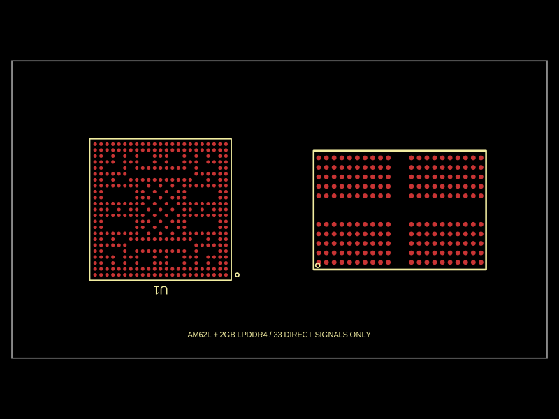 More from this author0hmX/simplified-am62l-computerThis code defines components and scripts for physically representing and routing high-speed DDR memory signals, power lines, and ground planes on an 8-layer PCB with detailed pin assignments, copper pours, and precise via and trace layouts based on TI EVM reference data.
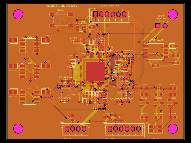 Similar packageseveibar/f1c100s-dev-boardThis code defines the hardware layout and schematic for a four-layer F1C100S-based module, including footprint placement, pin mappings, power regulation, decoupling capacitors, support components, and routing configurations, enabling automated PCB generation, routing, and verification.
 Discover something newhrithik18k/smart-switch-pcbThe AO3400A component models a SOT-23 N-channel MOSFET with labeled pins for Gate, Source, and Drain, including 3D CAD models and schematic symbols for electronic circuit design.