0hmX/robocraze-ov7670-camera-module-clone
This code defines and generates a 4-layer PCB hardware layout featuring an OV7670 VGA camera sensor module with fixed component placement, power regulation using ME6211 voltage regulators, a 2x9 header interface, and associated signal routing and mechanical footprints, designed for manufacturing and assembly.
- Version
- 1.0.7
- License
- MIT
- Stars
- 0
boards/RobocrazeOV7670CameraModuleBoard.tsx
import { Fragment } from "react"
import {
AutoroutingPipelineSolver,
type SimpleRouteJson as CapacitySimpleRouteJson,
} from "@tscircuit/capacity-autorouter"
import type {
AutorouterCompleteEvent,
AutorouterErrorEvent,
AutorouterProgressEvent,
GenericLocalAutorouter,
SimpleRouteJson,
SimplifiedPcbTrace,
} from "tscircuit"
import { OV7670ModuleHeader } from "../components/OV7670ModuleHeader"
import { OV7670Sensor } from "../components/OV7670Sensor"
import { ME6211C18M5G_N } from "../imports/ME6211C18M5G_N"
import { ME6211C28M5G_N } from "../imports/ME6211C28M5G_N"
const INPUT_POWER = "input_and_2v8_power"
const CORE_POWER = "core_1v8_power"
const SENSOR = "ov7670_sensor"
const ANALOG_RAILS = "sensor_analog_and_reference"
const IO_RAIL = "sensor_io_power"
const INTERFACE = "camera_interface"
const DNP = "dnp"
const parts = {
c100n: { jlcpcb: ["C14663"], mpn: "CC0603KRX7R9BB104" },
c1u: { jlcpcb: ["C15849"], mpn: "CL10A105KB8NNNC" },
c4u7: { jlcpcb: ["C19666"], mpn: "CL10A475KO8NNNC" },
c10u: { jlcpcb: ["C19702"], mpn: "CL10A106KP8NNNC" },
r10: { jlcpcb: ["C22859"], mpn: "0603WAF100JT5E" },
r0: { jlcpcb: ["C21189"], mpn: "0603WAF0000T5E" },
r1k: { jlcpcb: ["C21190"], mpn: "0603WAF1001T5E" },
r10k: { jlcpcb: ["C2906982"], mpn: "FRC0603F1002TS" },
ledRed: { jlcpcb: ["C2286"], mpn: "KT-0603R" },
}
const headerPairs = [
["3V3", "GND"],
["SIOC", "SIOD"],
["VSYNC", "HREF"],
["PCLK", "XCLK"],
["D7", "D6"],
["D5", "D4"],
["D3", "D2"],
["D1", "D0"],
["RESET#", "PWDN"],
] as const
const directSignals = [
"SIO_C",
"VSYNC",
"HREF",
"PCLK",
"XCLK",
"D7",
"D6",
"D5",
"D4",
"D3",
"D2",
"D1",
"D0",
"PWDN",
] as const
const schematicSignalLabels: Record<(typeof directSignals)[number], string> = {
SIO_C: "SCCB_SCL",
VSYNC: "VSYNC",
HREF: "HREF",
PCLK: "PCLK",
XCLK: "XCLK",
D7: "D7",
D6: "D6",
D5: "D5",
D4: "D4",
D3: "D3",
D2: "D2",
D1: "D1",
D0: "D0",
PWDN: "PWDN",
}
/**
* Reserve the demonstrated 0.10 mm CSP escapes before whole-board routing.
* XCLK and VREF1 hand off to the router after a through-via. HREF uses a fixed
* 0.15 mm bottom route after its 0.10 mm ball-field escape because the automatic
* HREF route otherwise misses the neighboring DOVDD clearance by 0.006 mm.
*/
const prepareReservedCspRoutes = (simpleRouteJson: SimpleRouteJson) => {
const input = structuredClone(
simpleRouteJson,
) as unknown as CapacitySimpleRouteJson
const xclkConnection = input.connections.find((connection) =>
connection.pointsToConnect.some(
(point) => Math.hypot(point.x - 3, point.y + 0.93) < 0.2,
),
)
const sensorPoint = xclkConnection?.pointsToConnect.find(
(point) => Math.hypot(point.x - 3, point.y + 0.93) < 0.2,
)
if (!xclkConnection || !sensorPoint) {
return {
input,
preexistingTraces: [] as SimplifiedPcbTrace[],
}
}
const breakoutPointId = "XCLK_CSP_BREAKOUT_BOTTOM"
const originalPortId = sensorPoint.pcb_port_id
xclkConnection.pointsToConnect = xclkConnection.pointsToConnect.map((point) =>
point === sensorPoint
? {
x: 6,
y: -2.5,
layer: "bottom",
pointId: breakoutPointId,
}
: point,
)
const xclkDogbone = {
type: "pcb_trace",
pcb_trace_id: "XCLK_CSP_DOGBONE",
connection_name: xclkConnection.name,
connectsTo: [originalPortId, breakoutPointId].filter(
(value): value is string => Boolean(value),
),
route: [
{
route_type: "wire",
x: 3,
y: -0.93,
width: 0.1,
layer: "top",
start_pcb_port_id: originalPortId,
},
{ route_type: "wire", x: 3, y: -0.31, width: 0.1, layer: "top" },
{ route_type: "wire", x: 6, y: -0.31, width: 0.1, layer: "top" },
{ route_type: "wire", x: 6, y: -2.5, width: 0.1, layer: "top" },
{
route_type: "via",
x: 6,
y: -2.5,
from_layer: "top",
to_layer: "bottom",
via_diameter: 0.45,
via_hole_diameter: 0.2,
},
{ route_type: "wire", x: 6, y: -2.5, width: 0.1, layer: "bottom" },
],
} as unknown as SimplifiedPcbTrace
const vref1Connection = input.connections.find((connection) =>
connection.pointsToConnect.some(
(point) => Math.hypot(point.x - 2.38, point.y - 0.31) < 0.2,
),
)
const vref1SensorPoint = vref1Connection?.pointsToConnect.find(
(point) => Math.hypot(point.x - 2.38, point.y - 0.31) < 0.2,
)
const reservedTraces = [xclkDogbone]
if (vref1Connection && vref1SensorPoint) {
const vref1BreakoutPointId = "VREF1_CSP_BREAKOUT_BOTTOM"
const vref1PortId = vref1SensorPoint.pcb_port_id
vref1Connection.pointsToConnect = vref1Connection.pointsToConnect.map(
(point) =>
point === vref1SensorPoint
? {
x: 5.2,
y: 0.5,
layer: "bottom",
pointId: vref1BreakoutPointId,
}
: point,
)
reservedTraces.push({
type: "pcb_trace",
pcb_trace_id: "VREF1_CSP_DOGBONE",
connection_name: vref1Connection.name,
connectsTo: [vref1PortId, vref1BreakoutPointId].filter(
(value): value is string => Boolean(value),
),
route: [
{
route_type: "wire",
x: 2.38,
y: 0.31,
width: 0.1,
layer: "top",
start_pcb_port_id: vref1PortId,
},
{ route_type: "wire", x: 2.69, y: 0, width: 0.1, layer: "top" },
{ route_type: "wire", x: 5.2, y: 0, width: 0.1, layer: "top" },
{ route_type: "wire", x: 5.2, y: 0.5, width: 0.1, layer: "top" },
{
route_type: "via",
x: 5.2,
y: 0.5,
from_layer: "top",
to_layer: "bottom",
via_diameter: 0.45,
via_hole_diameter: 0.2,
},
{ route_type: "wire", x: 5.2, y: 0.5, width: 0.1, layer: "bottom" },
],
} as unknown as SimplifiedPcbTrace)
}
const hrefConnection = input.connections.find((connection) =>
connection.pointsToConnect.some(
(point) => Math.hypot(point.x - 2.38, point.y + 0.31) < 0.2,
),
)
const hrefSensorPoint = hrefConnection?.pointsToConnect.find(
(point) => Math.hypot(point.x - 2.38, point.y + 0.31) < 0.2,
)
const hrefHeaderPoint = hrefConnection?.pointsToConnect.find(
(point) => point !== hrefSensorPoint,
)
if (hrefConnection && hrefSensorPoint && hrefHeaderPoint) {
const hrefPortId = hrefSensorPoint.pcb_port_id
const hrefHeaderPortId = hrefHeaderPoint.pcb_port_id
input.connections = input.connections.filter(
(connection) => connection !== hrefConnection,
)
reservedTraces.push({
type: "pcb_trace",
pcb_trace_id: "HREF_CSP_ESCAPE_AND_HEADER_ROUTE",
connection_name: hrefConnection.name,
connectsTo: [hrefPortId, hrefHeaderPortId].filter(
(value): value is string => Boolean(value),
),
route: [
{
route_type: "wire",
x: 2.38,
y: -0.31,
width: 0.1,
layer: "top",
start_pcb_port_id: hrefPortId,
},
{ route_type: "wire", x: 2.07, y: -0.62, width: 0.1, layer: "top" },
{ route_type: "wire", x: 0.5, y: -0.62, width: 0.1, layer: "top" },
{
route_type: "via",
x: 0.5,
y: -0.62,
from_layer: "top",
to_layer: "bottom",
via_diameter: 0.45,
via_hole_diameter: 0.2,
},
{ route_type: "wire", x: 0.5, y: -0.62, width: 0.15, layer: "bottom" },
{ route_type: "wire", x: 0.5, y: -8.5, width: 0.15, layer: "bottom" },
{ route_type: "wire", x: -9.5, y: -8.5, width: 0.15, layer: "bottom" },
{
route_type: "wire",
x: -9.5,
y: hrefHeaderPoint.y,
width: 0.15,
layer: "bottom",
},
{
route_type: "wire",
x: hrefHeaderPoint.x,
y: hrefHeaderPoint.y,
width: 0.15,
layer: "bottom",
end_pcb_port_id: hrefHeaderPortId,
},
],
} as unknown as SimplifiedPcbTrace)
}
input.traces = [
...(input.traces ?? []),
...(reservedTraces as unknown as NonNullable<
CapacitySimpleRouteJson["traces"]
>),
]
return { input, preexistingTraces: reservedTraces }
}
class ThroughViaOnlyAutorouter implements GenericLocalAutorouter {
input: SimpleRouteJson
isRouting = false
private solver: AutoroutingPipelineSolver
private preexistingTraces: SimplifiedPcbTrace[]
private timeoutId?: ReturnType<typeof setTimeout>
private eventHandlers = {
complete: [] as Array<(event: AutorouterCompleteEvent) => void>,
error: [] as Array<(event: AutorouterErrorEvent) => void>,
progress: [] as Array<(event: AutorouterProgressEvent) => void>,
}
constructor(simpleRouteJson: SimpleRouteJson) {
const prepared = prepareReservedCspRoutes(simpleRouteJson)
this.preexistingTraces = prepared.preexistingTraces
this.input = {
...prepared.input,
// Preserve inner1/inner2 as uninterrupted power/ground plane layers.
// The automatic router may use top and bottom and ordinary through-vias.
layerCount: 2,
allowViaInPad: false,
// Leave manufacturing margin around CSP lands. The core checker requires
// 0.10 mm; asking the router for 0.15 mm prevents borderline rounded
// geometry from being emitted below that limit.
minViaEdgeToPadEdgeClearance: 0.15,
} as unknown as SimpleRouteJson
this.solver = new AutoroutingPipelineSolver(this.input as unknown as CapacitySimpleRouteJson)
}
start() {
if (this.isRouting) return
this.isRouting = true
this.runCycle()
}
stop() {
this.isRouting = false
if (this.timeoutId !== undefined) clearTimeout(this.timeoutId)
}
on(event: "complete", callback: (event: AutorouterCompleteEvent) => void): void
on(event: "error", callback: (event: AutorouterErrorEvent) => void): void
on(event: "progress", callback: (event: AutorouterProgressEvent) => void): void
on(
event: "complete" | "error" | "progress",
callback:
| ((event: AutorouterCompleteEvent) => void)
| ((event: AutorouterErrorEvent) => void)
| ((event: AutorouterProgressEvent) => void),
) {
;(this.eventHandlers[event] as Array<typeof callback>).push(callback)
}
solveSync(): SimplifiedPcbTrace[] {
this.solver.solve()
if (this.solver.failed) {
throw new Error(this.solver.error ?? "Through-via-only autorouting failed")
}
return [
...this.preexistingTraces,
...((this.solver.getOutputSimpleRouteJson().traces ?? []) as unknown as SimplifiedPcbTrace[]),
]
}
getOutputSimpleRouteJson() {
const output = this.solver.getOutputSimpleRouteJson()
return {
...output,
traces: [
...this.preexistingTraces,
...((output.traces ?? []) as unknown as SimplifiedPcbTrace[]),
],
} as unknown as SimpleRouteJson
}
private runCycle = () => {
if (!this.isRouting) return
try {
const startedAt = Date.now()
const startingIterations = this.solver.iterations
while (
Date.now() - startedAt < 200 &&
!this.solver.solved &&
!this.solver.failed
) {
this.solver.step()
}
if (this.solver.failed) {
this.isRouting = false
const error = new Error(
this.solver.error ?? "Through-via-only autorouting failed",
)
for (const handler of this.eventHandlers.error) {
handler({ type: "error", error })
}
return
}
if (this.solver.solved) {
this.isRouting = false
const traces = [
...this.preexistingTraces,
...((this.solver.getOutputSimpleRouteJson().traces ??
[]) as unknown as SimplifiedPcbTrace[]),
]
for (const handler of this.eventHandlers.complete) {
handler({ type: "complete", traces })
}
return
}
const elapsedMs = Math.max(1, Date.now() - startedAt)
const iterationsPerSecond =
((this.solver.iterations - startingIterations) / elapsedMs) * 1000
for (const handler of this.eventHandlers.progress) {
handler({
type: "progress",
steps: this.solver.iterations,
progress: this.solver.progress,
phase: this.solver.getCurrentPhase(),
iterationsPerSecond,
})
}
this.timeoutId = setTimeout(this.runCycle, 0)
} catch (caught) {
this.isRouting = false
const error = caught instanceof Error ? caught : new Error(String(caught))
for (const handler of this.eventHandlers.error) {
handler({ type: "error", error })
}
}
}
}
const createThroughViaOnlyAutorouter = async (simpleRouteJson: SimpleRouteJson) =>
new ThroughViaOnlyAutorouter(simpleRouteJson)
function NamedTrace({
from,
to,
label,
routingPhaseIndex,
maxLength,
width,
}: {
from: string
to: string
label?: string
routingPhaseIndex?: number
maxLength?: string
width?: string
}) {
const clean = (value: string) => value.replace(/[^a-zA-Z0-9]+/g, "_")
const connectedNet = [from, to].find((value) => value.startsWith("net."))
const schematicLabel = label ?? connectedNet?.slice(4)
// Perimeter placement intentionally makes several reference and decoupling
// connections longer than the JSX default. Physical quality is validated
// after autorouting instead of using a pre-route straight-line veto.
const effectiveMaxLength = maxLength ?? "100mm"
return (
<trace
name={`${clean(from)}_TO_${clean(to)}`}
from={from}
to={to}
schDisplayLabel={schematicLabel}
routingPhaseIndex={routingPhaseIndex}
maxLength={effectiveMaxLength}
width={width}
/>
)
}
/**
* Standalone FIFO-less OV7670 module matching the B0FDRCHSFW interface.
* Component placement is fixed; PCB traces are generated by the autorouter.
*/
export function RobocrazeOV7670CameraModuleBoard() {
return (
<board
name="ROBOCRAZE_OV7670_CAMERA_MODULE"
title="Electrobot OV7670 VGA Camera Module Interface Clone"
width="35.16mm"
height="34.29mm"
layers={4}
thickness="1.6mm"
borderRadius="0.5mm"
solderMaskColor="blue"
silkscreenColor="white"
doubleSidedAssembly
autorouter={{ local: true, algorithmFn: createThroughViaOnlyAutorouter }}
schTraceAutoLabelEnabled
defaultTraceWidth="0.15mm"
nominalTraceWidth="0.15mm"
minTraceWidth="0.1mm"
minTraceToPadEdgeClearance="0.1mm"
minViaEdgeToPadEdgeClearance="0.1mm"
minViaHoleEdgeToViaHoleEdgeClearance="0.2mm"
minViaHoleDiameter="0.2mm"
minViaPadDiameter="0.45mm"
minBoardEdgeClearance="0.3mm"
>
<schematicsheet
name="main"
displayName="OV7670 standalone camera module"
sheetIndex={0}
>
<schematicsection
name={INPUT_POWER}
displayName="POWER INPUT + 2.8 V ANALOG / I/O SUPPLY"
/>
<schematicsection
name={CORE_POWER}
displayName="1.8 V SENSOR CORE SUPPLY"
/>
<schematicsection name={SENSOR} displayName="OV7670 IMAGE SENSOR" />
<schematicsection
name={ANALOG_RAILS}
displayName="AVDD + ANALOG REFERENCE FILTERING"
/>
<schematicsection
name={IO_RAIL}
displayName="DOVDD 2.8 V SENSOR I/O FILTERING"
/>
<schematicsection
name={INTERFACE}
displayName="CAMERA HEADER / DVP / SCCB CONTROL"
/>
<schematicsection
name={DNP}
displayName="OPTIONAL POWER INDICATOR — DO NOT POPULATE"
/>
</schematicsheet>
<group name="MAIN_SHEET_CONTENT" schSheetName="main">
{[
"V3V3",
"V2V8",
"AVDD",
"DOVDD",
"AGND",
"GND",
"RESET_N",
"VREF1",
"VREF2",
"DNP_LED_A",
].map((name) => (
<Fragment key={name}>
<net name={name} />
</Fragment>
))}
<copperpour
name="V2V8_POUR_INNER1"
layer="inner1"
connectsTo="net.V2V8"
clearance="0.3mm"
padMargin="0.3mm"
traceMargin="0.3mm"
boardEdgeMargin="0.3mm"
cutoutMargin="0.3mm"
useThermalReliefs
coveredWithSolderMask
/>
<copperpour
name="GND_POUR_INNER2"
layer="inner2"
connectsTo="net.GND"
clearance="0.3mm"
padMargin="0.3mm"
traceMargin="0.3mm"
boardEdgeMargin="0.3mm"
cutoutMargin="0.3mm"
useThermalReliefs
coveredWithSolderMask
/>
<hole name="H1" pcbX={-14.765} pcbY={14.235} diameter="2.5mm" />
<hole name="H2" pcbX={14.765} pcbY={14.235} diameter="2.5mm" />
<hole name="H3" pcbX={-14.765} pcbY={-14.235} diameter="2.5mm" />
<hole name="H4" pcbX={14.765} pcbY={-14.235} diameter="2.5mm" />
<OV7670ModuleHeader
name="J1"
displayName="2x9 CAMERA HEADER"
layer="bottom"
pcbX={-12.5}
pcbY={0}
pcbRotation={-90}
schSectionName={INTERFACE}
schX={11}
schY={2}
schWidth={2.15}
schHeight={2}
schPinArrangement={{
leftSide: {
pins: ["3V3", "SIO_C", "VSYNC", "PCLK", "D7", "D5", "D3", "D1", "RESET"],
direction: "top-to-bottom",
},
rightSide: {
pins: ["GND", "SIO_D", "HREF", "XCLK", "D6", "D4", "D2", "D0", "PWDN"],
direction: "top-to-bottom",
},
}}
/>
<ME6211C28M5G_N
name="U1"
displayName="2.8 V LDO"
layer="bottom"
pcbX={-4}
pcbY={12}
pcbRotation={90}
schSectionName={INPUT_POWER}
schX={-9}
schY={5.5}
schWidth={1.6}
schHeight={0.6}
schPinArrangement={{
leftSide: { pins: ["VIN", "CE"], direction: "top-to-bottom" },
rightSide: { pins: ["VOUT", "VSS"], direction: "top-to-bottom" },
}}
/>
<ME6211C18M5G_N
name="U2"
displayName="1.8 V LDO"
layer="bottom"
pcbX={6.5}
pcbY={-12}
pcbRotation={90}
schSectionName={CORE_POWER}
schX={-9}
schY={-4.5}
schWidth={1.6}
schHeight={0.6}
schPinArrangement={{
leftSide: { pins: ["VIN", "CE"], direction: "top-to-bottom" },
rightSide: { pins: ["VOUT", "VSS"], direction: "top-to-bottom" },
}}
/>
<capacitor
name="C1"
displayName="3V3 input bulk"
capacitance="4.7uF"
footprint="0603"
manufacturerPartNumber={parts.c4u7.mpn}
supplierPartNumbers={{ jlcpcb: parts.c4u7.jlcpcb }}
layer="bottom"
pcbX={-7.5}
pcbY={10.7}
schSectionName={INPUT_POWER}
schX={-12}
schY={2.5}
schOrientation="vertical"
/>
<capacitor
name="C2"
displayName="2V8 output bulk"
capacitance="10uF"
footprint="0603"
manufacturerPartNumber={parts.c10u.mpn}
supplierPartNumbers={{ jlcpcb: parts.c10u.jlcpcb }}
layer="bottom"
pcbX={-0.5}
pcbY={13.3}
pcbRotation={180}
schSectionName={INPUT_POWER}
schX={-8}
schY={2.5}
schOrientation="vertical"
/>
<capacitor
name="C3"
displayName="2V8 output bypass"
capacitance="1uF"
footprint="0603"
manufacturerPartNumber={parts.c1u.mpn}
supplierPartNumbers={{ jlcpcb: parts.c1u.jlcpcb }}
layer="bottom"
pcbX={2.8}
pcbY={13.3}
pcbRotation={180}
schSectionName={INPUT_POWER}
schX={-5.5}
schY={2.5}
schOrientation="vertical"
/>
<capacitor
name="C5"
displayName="1V8 regulator input"
capacitance="10uF"
footprint="0603"
manufacturerPartNumber={parts.c10u.mpn}
supplierPartNumbers={{ jlcpcb: parts.c10u.jlcpcb }}
layer="bottom"
pcbX={10}
pcbY={-13.3}
pcbRotation={180}
schSectionName={CORE_POWER}
schX={-12.5}
schY={-7}
schOrientation="vertical"
/>
<capacitor
name="C6"
displayName="1V8 output bypass"
capacitance="1uF"
footprint="0603"
manufacturerPartNumber={parts.c1u.mpn}
supplierPartNumbers={{ jlcpcb: parts.c1u.jlcpcb }}
layer="bottom"
pcbX={3}
pcbY={-10.7}
schSectionName={CORE_POWER}
schX={-9.3}
schY={-7}
schOrientation="vertical"
/>
<OV7670Sensor
name="U3"
displayName="OV7670 image sensor (CSP2)"
pcbX={3}
pcbY={0}
schSectionName={SENSOR}
schX={1}
schY={1.5}
schWidth={2.245}
schHeight={2.6}
schPinArrangement={{
leftSide: {
pins: ["AVDD", "DOVDD", "DVDD", "AGND", "DOGND", "VREF1", "VREF2", "SIO_C", "SIO_D", "XCLK", "RESET_N", "PWDN"],
direction: "top-to-bottom",
},
rightSide: {
pins: ["PCLK", "VSYNC", "HREF", "D7", "D6", "D5", "D4", "D3", "D2", "D1", "D0", "STROBE"],
direction: "top-to-bottom",
},
}}
noConnect={["STROBE"]}
/>
<resistor
name="R1"
displayName="AVDD 10Ω filter"
resistance="10ohm"
footprint="0603"
manufacturerPartNumber={parts.r10.mpn}
supplierPartNumbers={{ jlcpcb: parts.r10.jlcpcb }}
layer="bottom"
pcbX={9.4}
pcbY={10.7}
pcbRotation={180}
schSectionName={ANALOG_RAILS}
schX={-3}
schY={6.2}
/>
<resistor
name="R2"
displayName="DOVDD 10Ω filter"
resistance="10ohm"
footprint="0603"
manufacturerPartNumber={parts.r10.mpn}
supplierPartNumbers={{ jlcpcb: parts.r10.jlcpcb }}
layer="bottom"
pcbX={-6.9}
pcbY={-10.7}
pcbRotation={180}
schSectionName={IO_RAIL}
schX={-3.5}
schY={-4}
/>
<resistor
name="R3"
displayName="AGND–GND star link"
resistance="0ohm"
footprint="0603"
manufacturerPartNumber={parts.r0.mpn}
supplierPartNumbers={{ jlcpcb: parts.r0.jlcpcb }}
layer="bottom"
pcbX={14.3}
pcbY={0}
pcbRotation={90}
schSectionName={ANALOG_RAILS}
schX={8}
schY={4.2}
/>
<capacitor name="C8" displayName="2V8 rail bulk" capacitance="10uF" footprint="0603" manufacturerPartNumber={parts.c10u.mpn} supplierPartNumbers={{ jlcpcb: parts.c10u.jlcpcb }} layer="bottom" pcbX={6.1} pcbY={10.7} schSectionName={ANALOG_RAILS} schX={-6} schY={6.2} schOrientation="vertical" />
<capacitor name="C9" displayName="DOVDD high-frequency bypass" capacitance="100nF" footprint="0603" manufacturerPartNumber={parts.c100n.mpn} supplierPartNumbers={{ jlcpcb: parts.c100n.jlcpcb }} layer="bottom" pcbX={-3.6} pcbY={-10.7} pcbRotation={180} schSectionName={IO_RAIL} schX={0} schY={-4} schOrientation="vertical" />
<capacitor name="C10" displayName="DVDD bulk" capacitance="4.7uF" footprint="0603" manufacturerPartNumber={parts.c4u7.mpn} supplierPartNumbers={{ jlcpcb: parts.c4u7.jlcpcb }} layer="bottom" pcbX={3} pcbY={-13.3} schSectionName={CORE_POWER} schX={-6.6} schY={-7} schOrientation="vertical" />
<capacitor name="C11" displayName="DVDD rail bypass" capacitance="100nF" footprint="0603" manufacturerPartNumber={parts.c100n.mpn} supplierPartNumbers={{ jlcpcb: parts.c100n.jlcpcb }} layer="bottom" pcbX={-0.3} pcbY={-13.3} schSectionName={CORE_POWER} schX={-3.9} schY={-7} schOrientation="vertical" />
<capacitor name="C12" displayName="AVDD high-frequency bypass" capacitance="100nF" footprint="0603" manufacturerPartNumber={parts.c100n.mpn} supplierPartNumbers={{ jlcpcb: parts.c100n.jlcpcb }} layer="bottom" pcbX={2} pcbY={10.7} schSectionName={ANALOG_RAILS} schX={0} schY={6.2} schOrientation="vertical" />
<capacitor name="C13" displayName="VREF1 bypass" capacitance="100nF" footprint="0603" manufacturerPartNumber={parts.c100n.mpn} supplierPartNumbers={{ jlcpcb: parts.c100n.jlcpcb }} layer="bottom" pcbX={-7.8} pcbY={1.5} pcbRotation={90} schSectionName={ANALOG_RAILS} schX={2} schY={4.2} schOrientation="vertical" />
<capacitor name="C14" displayName="VREF2 bypass" capacitance="100nF" footprint="0603" manufacturerPartNumber={parts.c100n.mpn} supplierPartNumbers={{ jlcpcb: parts.c100n.jlcpcb }} layer="bottom" pcbX={-7.8} pcbY={-1.5} pcbRotation={270} schSectionName={ANALOG_RAILS} schX={5} schY={4.2} schOrientation="vertical" />
<capacitor name="C15" displayName="DOVDD local bypass" capacitance="100nF" footprint="0603" manufacturerPartNumber={parts.c100n.mpn} supplierPartNumbers={{ jlcpcb: parts.c100n.jlcpcb }} layer="bottom" pcbX={10} pcbY={-10.7} pcbRotation={270} schSectionName={IO_RAIL} schX={6} schY={-4} schOrientation="vertical" />
<capacitor name="C16" displayName="DVDD sensor bypass" capacitance="100nF" footprint="0603" manufacturerPartNumber={parts.c100n.mpn} supplierPartNumbers={{ jlcpcb: parts.c100n.jlcpcb }} layer="bottom" pcbX={-0.3} pcbY={-10.7} schSectionName={CORE_POWER} schX={-1.2} schY={-7} schOrientation="vertical" />
<capacitor name="C17" displayName="AVDD bulk" capacitance="4.7uF" footprint="0603" manufacturerPartNumber={parts.c4u7.mpn} supplierPartNumbers={{ jlcpcb: parts.c4u7.jlcpcb }} layer="bottom" pcbX={12.7} pcbY={10.7} schSectionName={ANALOG_RAILS} schX={3} schY={6.2} schOrientation="vertical" />
<capacitor name="C18" displayName="DOVDD bulk" capacitance="4.7uF" footprint="0603" manufacturerPartNumber={parts.c4u7.mpn} supplierPartNumbers={{ jlcpcb: parts.c4u7.jlcpcb }} layer="bottom" pcbX={-6.9} pcbY={-13.3} schSectionName={IO_RAIL} schX={3} schY={-4} schOrientation="vertical" />
<resistor
name="R4"
displayName="SCCB SDA series protection"
resistance="1kohm"
footprint="0603"
manufacturerPartNumber={parts.r1k.mpn}
supplierPartNumbers={{ jlcpcb: parts.r1k.jlcpcb }}
layer="bottom"
pcbX={-10.2}
pcbY={-13.3}
schSectionName={INTERFACE}
schX={7}
schY={-2.5}
/>
<resistor
name="R5"
displayName="RESET# pull-up"
resistance="10kohm"
footprint="0603"
manufacturerPartNumber={parts.r10k.mpn}
supplierPartNumbers={{ jlcpcb: parts.r10k.jlcpcb }}
layer="bottom"
pcbX={14.3}
pcbY={-6.6}
pcbRotation={270}
schSectionName={INTERFACE}
schX={8.5}
schY={-4}
/>
<resistor
name="R0"
displayName="Power LED resistor (DNP)"
resistance="1kohm"
footprint="0603"
manufacturerPartNumber={parts.r1k.mpn}
supplierPartNumbers={{ jlcpcb: parts.r1k.jlcpcb }}
doNotPlace
pcbX={-9.6}
pcbY={14}
schSectionName={DNP}
schX={8}
schY={-7}
/>
<led
name="D0_IND"
displayName="Optional power LED (DNP)"
color="red"
footprint="0603"
manufacturerPartNumber={parts.ledRed.mpn}
supplierPartNumbers={{ jlcpcb: parts.ledRed.jlcpcb }}
doNotPlace
pcbX={-6.5}
pcbY={14}
schSectionName={DNP}
schX={12.5}
schY={-7}
/>
<NamedTrace from="J1.3V3" to="net.V3V3" width="0.3mm" />
<NamedTrace from="J1.GND" to="net.GND" width="0.3mm" />
{directSignals.map((signal) => (
<Fragment key={`header-${signal}`}>
<NamedTrace
from={`J1.${signal}`}
to={`U3.${signal}`}
label={schematicSignalLabels[signal]}
/>
</Fragment>
))}
<NamedTrace from="J1.SIO_D" to="R4.pin1" label="SCCB_SDA_HOST" />
<NamedTrace from="R4.pin2" to="U3.SIO_D" label="SCCB_SDA" />
<NamedTrace from="J1.RESET" to="U3.RESET_N" label="RESET_N" />
<NamedTrace from="U3.RESET_N" to="R5.pin1" label="RESET_N" />
<NamedTrace from="R5.pin2" to="C15.pin1" label="DOVDD_2V8" width="0.2mm" />
<NamedTrace from="U1.VIN" to="net.V3V3" width="0.3mm" />
<NamedTrace from="U1.CE" to="net.V3V3" width="0.3mm" />
<NamedTrace from="U1.VSS" to="net.GND" width="0.3mm" />
<NamedTrace from="U1.VOUT" to="C2.pin1" label="V2V8" width="0.25mm" />
<NamedTrace from="U1.VOUT" to="net.V2V8" width="0.25mm" />
<NamedTrace from="C1.pin1" to="net.V3V3" width="0.3mm" />
<NamedTrace from="C1.pin2" to="net.GND" width="0.3mm" />
<NamedTrace from="C2.pin2" to="net.GND" width="0.25mm" />
<NamedTrace from="C3.pin1" to="net.V2V8" width="0.25mm" />
<NamedTrace from="C3.pin2" to="net.GND" width="0.25mm" />
<NamedTrace from="U2.VIN" to="C5.pin1" label="V2V8" width="0.25mm" />
<NamedTrace from="U2.VIN" to="net.V2V8" width="0.25mm" />
<NamedTrace from="U2.CE" to="net.V2V8" width="0.25mm" />
<NamedTrace from="U2.VSS" to="net.GND" width="0.25mm" />
<NamedTrace from="U2.VOUT" to="C6.pin1" label="DVDD_1V8" width="0.25mm" />
<NamedTrace from="C5.pin2" to="net.GND" width="0.25mm" />
<NamedTrace from="C6.pin2" to="net.GND" width="0.25mm" />
<NamedTrace from="R1.pin1" to="C8.pin1" label="V2V8" width="0.25mm" />
<NamedTrace from="R1.pin1" to="net.V2V8" width="0.25mm" />
<NamedTrace from="R1.pin2" to="C12.pin1" label="AVDD" width="0.2mm" />
<NamedTrace from="R1.pin2" to="C17.pin1" label="AVDD" width="0.2mm" />
<NamedTrace from="C12.pin1" to="U3.AVDD" label="AVDD" width="0.2mm" />
<NamedTrace from="R2.pin1" to="net.V2V8" width="0.25mm" />
<NamedTrace from="R2.pin2" to="C9.pin1" label="DOVDD_2V8" width="0.2mm" />
<NamedTrace from="R2.pin2" to="C18.pin1" label="DOVDD_2V8" width="0.2mm" />
<NamedTrace from="C9.pin1" to="U3.DOVDD" label="DOVDD_2V8" width="0.2mm" />
<NamedTrace from="C6.pin1" to="C10.pin1" label="DVDD_1V8" width="0.25mm" />
<NamedTrace from="C10.pin1" to="C11.pin1" label="DVDD_1V8" width="0.2mm" />
<NamedTrace from="C11.pin1" to="C16.pin1" label="DVDD_1V8" width="0.2mm" />
<NamedTrace from="C16.pin1" to="U3.DVDD" label="DVDD_1V8" width="0.2mm" />
<NamedTrace from="U3.AGND" to="C13.pin2" label="AGND" width="0.2mm" />
<NamedTrace from="C13.pin2" to="C14.pin2" label="AGND" width="0.2mm" />
<NamedTrace from="C14.pin2" to="R3.pin1" label="AGND" width="0.2mm" />
<NamedTrace from="C13.pin2" to="C12.pin2" label="AGND" width="0.2mm" />
<NamedTrace from="C12.pin2" to="C17.pin2" label="AGND" width="0.2mm" />
<NamedTrace from="R3.pin2" to="net.GND" width="0.25mm" />
<NamedTrace from="U3.DOGND" to="net.GND" width="0.2mm" />
<NamedTrace from="U3.VREF1" to="C13.pin1" label="VREF1" />
<NamedTrace from="U3.VREF2" to="C14.pin1" label="VREF2" />
<NamedTrace from="C8.pin2" to="net.GND" width="0.25mm" />
<NamedTrace from="C9.pin1" to="C15.pin1" label="DOVDD_2V8" width="0.2mm" />
<NamedTrace from="C9.pin2" to="net.GND" width="0.2mm" />
<NamedTrace from="C10.pin2" to="net.GND" width="0.2mm" />
<NamedTrace from="C11.pin2" to="net.GND" width="0.2mm" />
<NamedTrace from="C15.pin2" to="net.GND" width="0.2mm" />
<NamedTrace from="C16.pin2" to="net.GND" width="0.2mm" />
<NamedTrace from="C18.pin2" to="net.GND" width="0.2mm" />
<NamedTrace from="R0.pin1" to="net.V3V3" />
<NamedTrace from="R0.pin2" to="net.DNP_LED_A" />
<NamedTrace from="D0_IND.anode" to="net.DNP_LED_A" />
<NamedTrace from="D0_IND.cathode" to="net.GND" />
{headerPairs.map(([left, right], pair) => {
const pcbY = 10.16 - pair * 2.54
return (
<Fragment key={`${left}-${right}`}>
<silkscreentext text={left} pcbX={-16.15} pcbY={pcbY} fontSize="0.42mm" anchorAlignment="center" />
<silkscreentext text={right} pcbX={-8.85} pcbY={pcbY} fontSize="0.42mm" anchorAlignment="center" />
</Fragment>
)
})}
<silkscreentext text="OV7670" pcbX={4} pcbY={15.4} fontSize="1mm" anchorAlignment="center" />
<silkscreentext text="3V3 PWR / 2V8 IO" pcbX={4} pcbY={-15.2} fontSize="1mm" anchorAlignment="center" />
<silkscreentext text="PIN 1" pcbX={-16.1} pcbY={11.8} fontSize="0.65mm" anchorAlignment="center" />
</group>
</board>
)
}
Related Packages
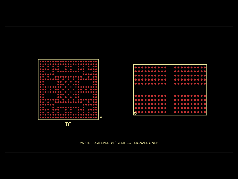 More from this author0hmX/simplified-am62l-computerThis code defines components and scripts for physically representing and routing high-speed DDR memory signals, power lines, and ground planes on an 8-layer PCB with detailed pin assignments, copper pours, and precise via and trace layouts based on TI EVM reference data.
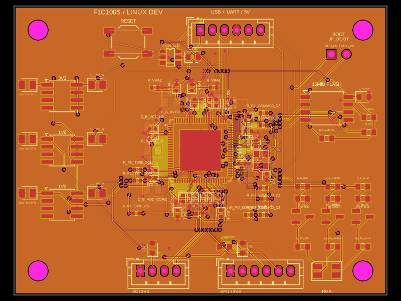 Similar packageseveibar/f1c100s-dev-boardThis code defines the hardware layout and schematic for a four-layer F1C100S-based module, including footprint placement, pin mappings, power regulation, decoupling capacitors, support components, and routing configurations, enabling automated PCB generation, routing, and verification.
 Discover something newhrithik18k/smart-switch-pcbThe AO3400A component models a SOT-23 N-channel MOSFET with labeled pins for Gate, Source, and Drain, including 3D CAD models and schematic symbols for electronic circuit design.